Huwin provides high-precision measurement of high-frequency signal transmission connectors, cables, and PCBs, as well as test fixture design/measurement and consulting services for this, based on ultra-high frequency engineering experience and patented technology.
PCB EMI Element Analysis
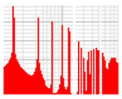
EMI signal source analysis - The fundamental element of EMI at the PCB level becomes the EMI signal source, the path through which the signal is transmitted, and the PCB pattern that plays the role of transmitting the signal to the outside like an antenna. The EMI signal source can be checked by identifying which frequency and magnitude of the signal is generated through the analysis of the circuit that causes the sudden change of current. First, the frequency characteristics of capacitor circuits and EMI filter circuits are analyzed to reduce signal noise and power noise generated by SMPS, digital clock signal and digital data signal generating circuits on the PCB.
EMI Pattern Analysis
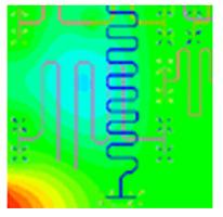
The PCB pattern adjacent to the EMI signal source, the pattern around the connector connected to the external cable, and the ground pattern around the SMPS should be designed to prevent coupling of high-frequency noise signals. By extracting the parasitic inductance and capacitance components of the PCB pattern, you can figure out how much signal is transmitted. This analysis can also provide solutions to the problem of signal interference inside the system as well as EMI to the outside of the system. EMI verification at the PCB level for high-frequency signals reduces the number of EMI debugging and trouble shooting at the system level, so it can be expected to shorten the development period and reduce the cost of EMI countermeasure parts.
EMI Radiator Analysis
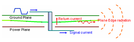
Resonance on the PCB and signal coupling of the resonant location is a major source of EMI as it acts like an antenna. In particular, for the wiring of the critical net containing high-frequency signal components, an appropriate design is required to prevent noise from radiating to the outside after analyzing the surrounding plane resonance. As the system gradually operates at high frequencies and becomes more complex, it is essential to analyze the noise element at the PCB level and design it in consideration of it in order to solve the problem of malfunction or instability due to interference within the system.
System level EMC/ESD Analysis
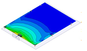
Cases such as structural or boundary conditions for the effect of shielding effect of system case through 3D EM analysis, noise coupling analysis in 3D structure adjacent to high frequency or high current
(high voltage) circuit, EMI/ESD gasket effect, heat sink effect, etc. We present a guide so that it can be applied to design by conducting a study.
The analysis result report includes not only recommended improvement measures for each problematic item,
but also technical background theory and training to help build a more efficient product development process in future designs.