Huwin provides high-precision measurement of high-frequency signal transmission connectors, cables, and PCBs, as well as test fixture design/measurement and consulting services for this, based on ultra-high frequency engineering experience and patented technology.
-
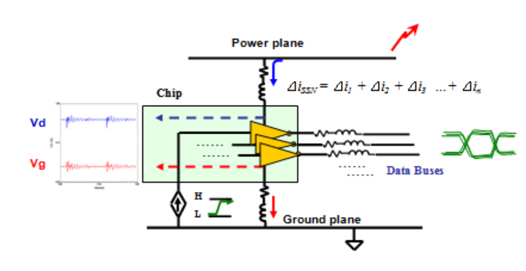
For the stable operation of the system, power integrity analysis has become an essential design process. Design through Power Integrity analysis is a way to reduce PCB noise, EMI and malfunction probability. In an equivalent circuit to the power bus that powers the IC, as shown on the right, ideally the transfer impedance between the Vdd pin and Vs of the device should be zero, and for DC it will be approximately zero.
However, if the frequency increases, the impedance between them increases. If a peak value of the impedance between them occurs, a voltage difference between the two nodes occurs. In other words, it means that the voltage drops from the power bus, and high voltage noise is generated in proportion to the transfer impedance. Transmission impedance can therefore be considered as an analysis parameter in Power Integrity analysis and is usually used as a design target parameter called Target Impedance.
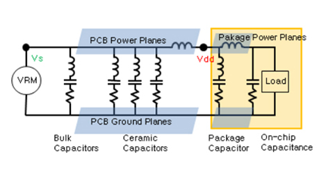
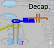
The most effective way to design the transfer impedance below the target impedance for stable power supply is to minimize the inductance of the power bus. A decoupling capacitor is used for this purpose. Since the noise generated by the clock frequency has a wide spectrum distribution and is distributed from several KHz to several GHz, capacitors of various values are required to reduce such wide bandwidth noise. However, the capacitor has no effect above several hundred MHz due to the parasitic inductance value of its packaging, and for frequencies above several hundred MHz, the capacitance component of the power side and the capacitance component of the package or on-die act as decoupling.
In Power Integrity analysis, noise analysis is performed in two ways. First, the transfer impedance is extracted as a result value for frequency by frequency sweep analysis, and then compared with the target impedance calculated from the specifications given in the data sheet.
-
The target impedance calculation is sometimes based on the maximum current, i.e. the condition when the current sinks are switched on in the same direction at the same time. Also, the switching frequency of the VRM that is directly operated on the power ground is important. Since it is in the range of several hundred KHz, it is a frequency that can be effectively suppressed by the bulk decoupling capacitor.
will indirectly affect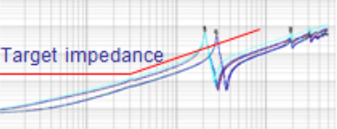
-
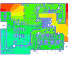
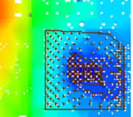
The second stage of noise analysis is resonance mode analysis. All power and ground planes have their own resonance mode due to their size, shape, and permittivity, and the frequency corresponding to the resonance mode is radiated to the outside by resonance even if the magnitude of the signal is not large, and may cause EMI problems. In the clock signal supplied by the power rail, care must be taken so that the higher-order harmonic component does not overlap the resonant frequency of the power plane, and the purpose of resonant mode analysis is to check whether the clock frequency and higher-order harmonic frequency overlap the mode frequency no see. In the resonant mode plot, the red and blue areas indicate the area where the noise magnitude peaks, and the IC placed in this area is affected by the frequency that requires attention, so the noise area of the resonant mode distribution has a Power Plain shape and Provides debugging information for IC placement or EMC trouble shooting. PDN analysis allows you to optimize the placement, type and ruler of decoupling capacitors. We will also perform Power Plain shape optimization for Core PDN, etc.
Power Delivery Network (PDN) optimization
Power/Ground Impedance / Resonance
Decap. Sensitivity / Loop Inductance
Decap. Optimization - Type/Number/Value/Cost
Core PDN optimization
PCB DC IR Drop Analysis
PCB current/voltage power loss distribution analysis
Power plane shape optimization for constant current distribution
System Level Power Integrity
Depending on the system characteristics and application,
the optimal PDN configuration should vary. In the case of a system that requires stability, it must be designed to satisfy very strict noise standards, and in the case of a general product, it must be
an efficient design that can lower the system price. In order to set the adaptive target impedance suitable for the characteristics of
the system, it is necessary to perform the overall circuit operation of the system to verify the analysis and influence of the noise level (SSN/SSO) in advance, and to apply it to the design. For this purpose, systematic analysis of IC/Package/PCB is performed.